Delay-Locked Loop
8 GHz, 15% jitter, 4% DCD, 6 mW, 45nm (schematic) with phase detector, charge pump, and delay-line
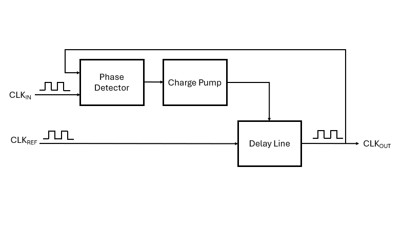
DLL-Based Clock Generation for Low-Jitter Synchronization
Abstract—This project focuses on the design of a Delay-Locked Loop (DLL) in a 45nm technology to generate a low-jitter clock signal phase-locked to a noisy input at 8.0 GHz. The DLL aims to minimize peak-to-peak jitter of the output clock under non-ideal conditions, including noise in the input signal and power supply. The DLL components, including a phase detector, loop filter, and delay line, were designed and simulated to achieve peak-to-peak jitter less than 25ps, duty-cycle distortion below 5%, and output voltage swing greater than 0.7V with a 1V supply. Simulations were conducted with and without noise components in the input signal and supply voltages, demonstrating the ability of the DLL to lock with low jitter across a range of input phase shifts. The design was optimized for minimal power consumption with stable locking, and the design meets the project specifications.
Phase Detector
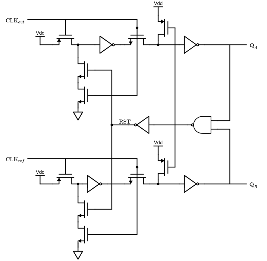
The phase detector consists of two resettable pass-transistor delay-flip flops (DFFs) [1]. An asynchronous reset sets the output low, and since the data input is tied high, the output will go high on the rising edge of the clock input. Once the output of both DFFs are high, they cause the NAND gate output to go low, thus causing a DFF reset. The outputs QA and QB will connect to the charge pump, allowing it to charge or discharge based on the phase mismatch between the inputs As the phase difference of the inputs decreases, so will the pulse width of the outputs on QA and QB. Ideally, the PFD will detect phase difference over a range of −2π to 2π, however, in a non-ideal design, a non-zero reset delay will cause cycle slipping and result in missed clock edges. In a properly designed system, there should be sufficient margin between the edges of the phase range and the desired phases for locking so that noise perturbations will not cause the system to lose its lock. To expand the range of phase detection without cycle slipping, the delay of the reset path must be minimized.
After implementing the circuit in Cadence, simulations were run, sweeping over various values of phase to verify a sufficient phase range. A linear region of \(\phi \in \text{[}-1.36\pi, 1.44\pi\text{]}\) gives a phase range of \(2.80\pi\), sufficiently exceeding the minimum required range of \(2\pi\).
Charge Pump
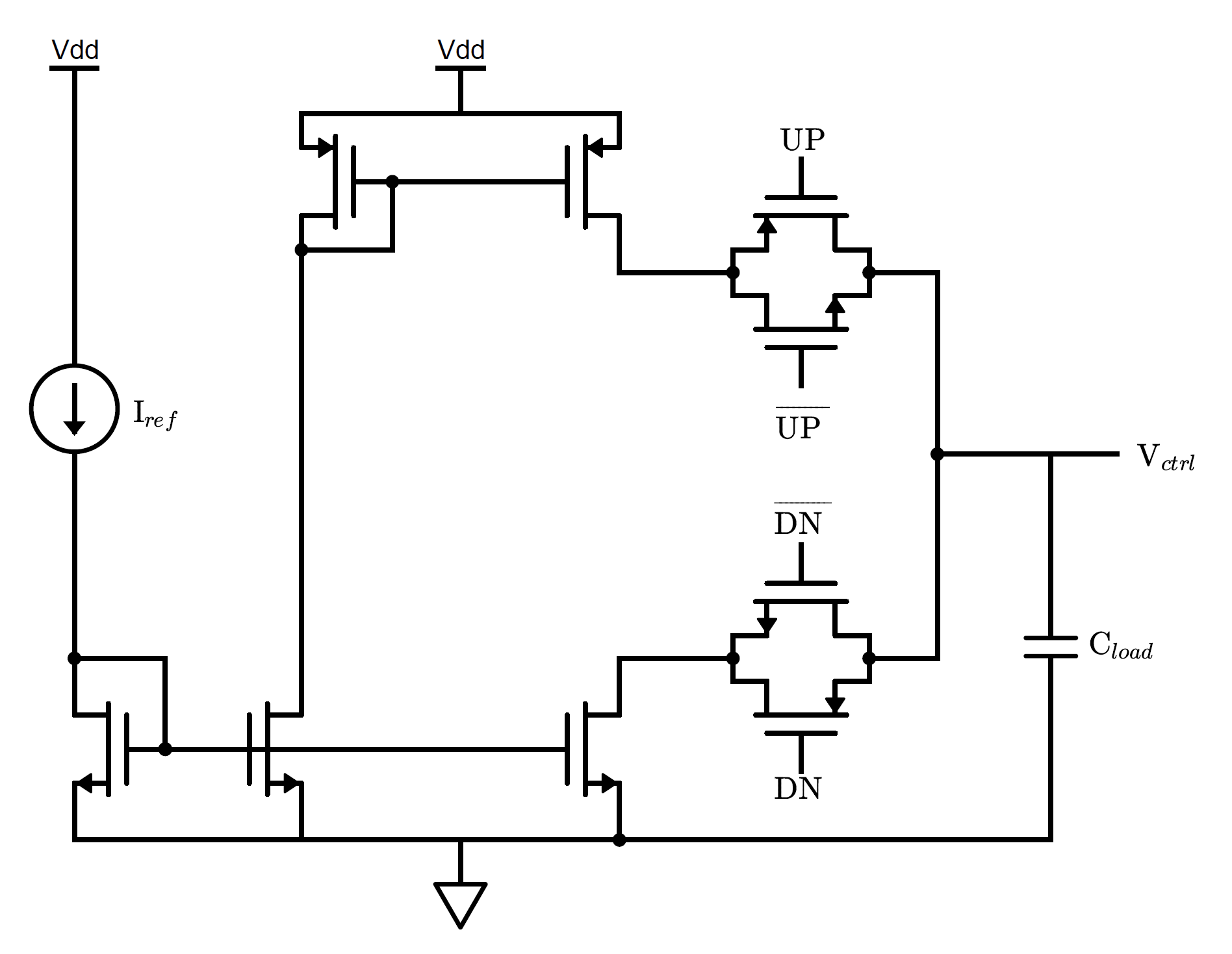
The charge pump acts as an integrator to generate an output voltage proportional to the phase detector output and was designed around an ideal 5uA current source provided in our design. The current source is used as the reference current for two current mirrors - one PMOS current mirror and one NMOS current mirror for up-charge and down-charge pump currents, respectively. Applying the current mirrors allows us to achieve a performance closer to an ideal current source at the output in terms of the current variation with output voltage. The current mirrors also allow for more flexibility in terms of the current values that can be controlled by adjusting transistor widths.
Complementary switches were adopted in our design to minimize charge injection, balancing out the gate charges. Switch transistors were designed with smaller width to mitigate charge sharing by reducing parasitic capacitances. The capacitance of the charge pump was selected to be 300fF for the same purpose of minimizing charge sharing and input voltage feedthrough from switches, while allowing for reasonable voltage swing at the output for the delay line.
Other transistor widths were modified to ensure up and down charge currents were equal and around \(60\mu A\). The design attempts to reduce the mismatch between currents to allow for smaller locking phase offset and \(V_{ctrl}\) ripple.
Delay Line
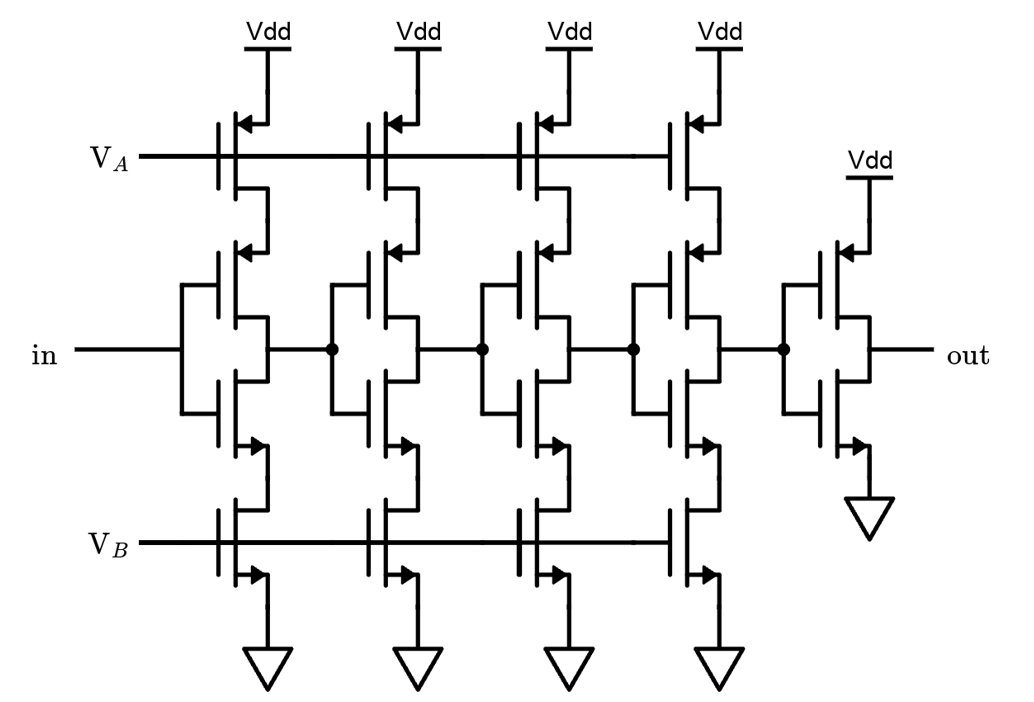
The delay line receives a clean 8 GHz reference clock as an input and adds delay so the phase matches between the input clock to the phase detector and the output of the delay line. The two control voltages (VA and VB) can provide a delay range of 125ps (\(2\pi\)). By connecting current-starved inverters in series the delay can be controlled by a control voltage. The current-starved inverters increase the rise and fall time, so an inverter is placed at the output of the delay element to reduce it. Additionally, proper sizing of the transistors was achieved to prevent more than 5% duty-cycle distortion (DCD) under noise in the system. The topology shown depicts 1 delayline element, and a total of 8 were used in series to achieve sufficient delay.
Performance Summary
The design was tested with and without noise. The power supply noise was 20mV 255 MHz oscillations and the clock input noise was 40mV oscillations at 7.845 GHz and 8.155 GHz. Under the worst case noise conditions, the following metrics were achieved (and compared with the design specifications required) at lock:
Power: 5.55mW < 8mW
Pk-pk Jitter: 14.1ps < 25ps
DCD: 4.5% < 5%
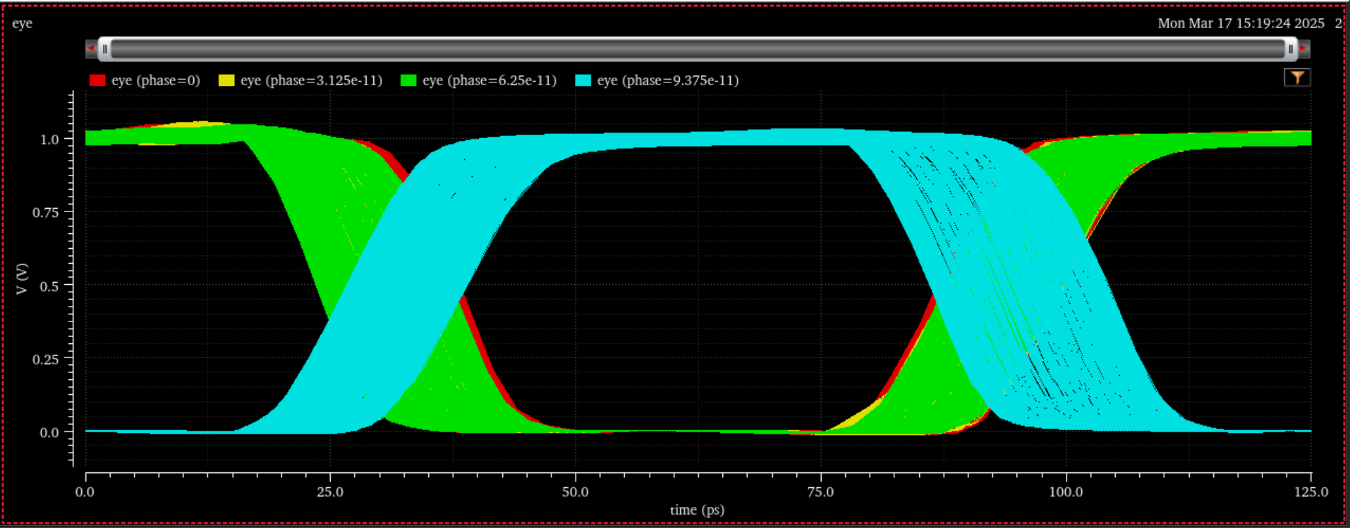 Overlapping eye diagrams of output clock for \(\phi=0,\pi/2,\pi,3\pi/2\)
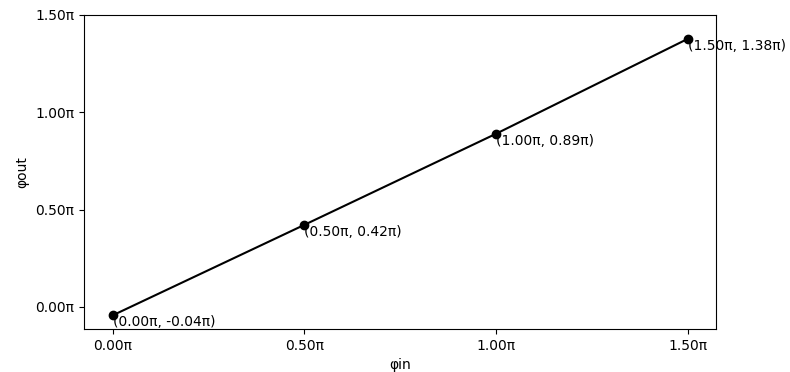 Comparison of phase of output clock relative to phase of input clock at lock
References
[1] M. Mansuri, D. Liu, and C.-K. K. Yang, “Fast frequency acquisition phase-frequency detectors for GSamples/s phase-locked loops,” IEEE J. Solid-State Circuits, vol. 37, no. 10, pp. 1331–1334, Oct. 2002.
[2] B. Razavi, “The delay-locked loop—A circuit for all seasons,” IEEE Solid-State Circuits Mag., vol. 10, no. 3, pp. 9–15, Summer 2018.